- 您现在的位置:买卖IC网 > Sheet目录1223 > KIT33996EKEVB (Freescale Semiconductor)KIT EVAL 33996 16OUTPUT SW W/SPI
�� �
�
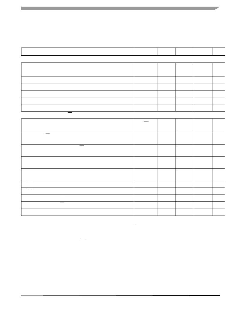
�ELECTRICAL� CHARACTERISTICS�
�DYNAMIC� ELECTRICAL� CHARACTERISTICS�
�DYNAMIC� ELECTRICAL� CHARACTERISTICS�
�Table� 4.� DYNAMIC� ELECTRICAL� CHARACTERISTICS�
�Characteristics� noted� under� conditions� of� 3.1� V� ≤� SO� PWR� ≤� 5.5� V,� 5.0� V� ≤� V� PWR� ≤� 18� V,� -40� °� C� ≤� T� A� ≤� 125� °� C� unless� otherwise�
�noted.� Where� applicable,� typical� values� reflect� the� parameter� ’s� approximate� average� value� with� V� PWR� =� 13� V,� T� A� =� 25� °� C.�
�Characteristic�
�Symbol�
�Min�
�Typ�
�Max�
�Unit�
�POWER� OUTPUT� TIMING� (VPWR)�
�Output� Slew� Rate�
�SR�
�V/� μ� s�
�R� L� =� 60� Ω�
�(15)�
�1.0�
�2.0�
�10�
�Output� Turn� ON� Delay� Time� (16)�
�t� DLY� (ON)�
�1.0�
�2.0�
�10�
�μ� s�
�Output� Turn� OFF� Delay� Time�
�(16)�
�t� DLY(OFF)�
�1.0�
�4.0�
�10�
�μ� s�
�Output� ON� Short� Fault� Disable� Report� Delay� (17)�
�t� DLY� (SHORT)�
�100�
�–�
�450�
�μ� s�
�Output� OFF� Open� Fault� Delay� Time�
�Output� PWM� Frequency�
�(17)�
�t� DLY(OPEN)�
�t� FREQ�
�100�
�–�
�–�
�–�
�450�
�2.0�
�μ� s�
�kHz�
�DIGITAL� INTERFACE� TIMING� (CS,� SO,� SI,� SCLK)� (23)�
�Required� Low� State� Duration� on� V� PWR� for� Reset�
�t� RST�
�μ� s�
�V� PWR� ≤� 0.2V� (18)�
�Falling� Edge� of� CS� to� Rising� Edge� of� SCLK�
�Required� Setup� Time�
�Falling� Edge� of� SCLK� to� Rising� Edge� of� CS�
�Required� Setup� Time�
�SI� to� Falling� Edge� of� SCLK�
�Required� Setup� Time�
�Falling� Edge� of� SCLK� to� SI�
�Required� Hold� Time�
�t� LEAD�
�t� LAG�
�t� SI� (su)�
�t� SI� (hold)�
�–�
�100�
�50�
�16�
�20�
�–�
�–�
�–�
�–�
�–�
�10�
�–�
�–�
�–�
�–�
�ns�
�ns�
�ns�
�ns�
�SI,� CS� ,� SCLK� Signal� Rise� Time� (19)�
�t� R� (SI)�
�–�
�5.0�
�–�
�ns�
�SI,� CS� ,� SCLK� Signal� Fall� Time�
�(19)�
�t� F� (SI)�
�–�
�5.0�
�–�
�ns�
�Time� from� Falling� Edge� of� CS� to� SO� Low-impedance� (20)�
�t� SO� (EN)�
�–�
�–�
�50�
�ns�
�Time� from� Rising� Edge� of� CS� to� SO� High-impedance�
�(21)�
�t� SO� (DIS)�
�–�
�–�
�50�
�ns�
�Time� from� Rising� Edge� of� SCLK� to� SO� Data� Valid� (22)�
�t� VALID�
�–�
�25�
�80�
�ns�
�Notes�
�15.�
�16.�
�17.�
�18.�
�19.�
�20.�
�21.�
�22.�
�23.�
�Output� slew� rate� measured� across� a� 60� Ω� resistive� load.�
�Output� turn� ON� and� OFF� delay� time� measured� from� 50%� rising� edge� of� CS� to� 80%� and� 20%� of� initial� voltage.�
�Duration� of� fault� before� fault� bit� is� set.� Duration� between� access� times� must� be� greater� than� 450� μ� s� to� read� faults.�
�This� parameter� is� guaranteed� by� design;� however,� it� is� not� production� tested.�
�Rise� and� Fall� time� of� incoming� SI,� CS� ,� and� SCLK� signals� suggested� for� design� consideration� to� prevent� the� occurrence� of� double� pulsing.�
�Time� required� for� valid� output� status� data� to� be� available� on� SO� pin.�
�Time� required� for� output� states� data� to� be� terminated� at� SO� pin.�
�Time� required� to� obtain� valid� data� out� from� SO� following� the� rise� of� SCLK� with� 200pF� load.�
�This� parameter� is� guaranteed� by� design.� Production� test� equipment� used� 4.16MHz,� 5.5/3.1V� SPI� Interface.�
�33996�
�Analog� Integrated� Circuit� Device� Data�
�Freescale� Semiconductor�
�7�
�发布紧急采购,3分钟左右您将得到回复。
相关PDF资料
KIT34673EPEVBE
KIT EVALUATION FOR MC34673
KIT34674EPEVBE
KIT EVAL BOARD 10CH LED BACKLGHT
KIT34675EPEVBE
KIT EVALUATION FOR MC34675
KIT35XS3500EVBE
KIT EVAL QUAD HIGH SIDE SWITCH
KITUSBSPIEVME
KIT EVAL USB-SPI W/MC68HC908JW32
KP3040
KEYPAD USB W/2 USB PORTS
KS8737-EVAL
BOARD EVAL EXPERIMENT FOR KS8737
KSZ8695PX-EVAL
KIT EVAL KSZ8695PX EXPERIMENT
相关代理商/技术参数
KIT33999EKEVB
功能描述:电源管理IC开发工具 33999 PDOSS EVAL KIT RoHS:否 制造商:Maxim Integrated 产品:Evaluation Kits 类型:Battery Management 工具用于评估:MAX17710GB 输入电压: 输出电压:1.8 V
KIT34670EGEVBE
功能描述:电源管理IC开发工具 IEEE 802.3AF PD WITH CUR RoHS:否 制造商:Maxim Integrated 产品:Evaluation Kits 类型:Battery Management 工具用于评估:MAX17710GB 输入电压: 输出电压:1.8 V
KIT34671EPEVBE
功能描述:电源管理IC开发工具 HIGH-INPUT-VOLT CHARGER RoHS:否 制造商:Maxim Integrated 产品:Evaluation Kits 类型:Battery Management 工具用于评估:MAX17710GB 输入电压: 输出电压:1.8 V
KIT34673EPEVBE
功能描述:电源管理IC开发工具 IC, HIGH-INPUT-VOLT CHARGER RoHS:否 制造商:Maxim Integrated 产品:Evaluation Kits 类型:Battery Management 工具用于评估:MAX17710GB 输入电压: 输出电压:1.8 V
KIT34674EPEVBE
功能描述:电源管理IC开发工具 IC, 10 CH LED BACKLIGHT RoHS:否 制造商:Maxim Integrated 产品:Evaluation Kits 类型:Battery Management 工具用于评估:MAX17710GB 输入电压: 输出电压:1.8 V
KIT34675EPEVBE
功能描述:电源管理IC开发工具 28V-INPUT-VOLT SNGL RoHS:否 制造商:Maxim Integrated 产品:Evaluation Kits 类型:Battery Management 工具用于评估:MAX17710GB 输入电压: 输出电压:1.8 V
KIT34676EPEVBE
功能描述:电源管理IC开发工具 DUAL 28V-INPUTVOLT C RoHS:否 制造商:Maxim Integrated 产品:Evaluation Kits 类型:Battery Management 工具用于评估:MAX17710GB 输入电压: 输出电压:1.8 V
KIT34676EPEVBE
制造商:Freescale Semiconductor 功能描述:Dual 28V input voltage single cell Li-Io